This article systematically breaks down the memory landscape, covering the performance differences and application boundaries of NOR Flash, NAND Flash, SSD/eMMC/UFS, as well as SRAM, DRAM, DDR, LPDDR, and GDDR. It addresses a common design challenge: how to choose the right medium for boot, runtime memory, and persistent storage. Keywords: memory, Flash, DRAM.
Technical Specification Snapshot
| Parameter | Information |
|---|---|
| Document Topic | Memory types and deployment selection |
| Domain | Embedded systems, computer architecture, firmware development |
| Language | Chinese |
| Protocols/Interfaces Involved | SPI, SATA, NVMe, eMMC, UFS, DDR |
| Stars | N/A (original content is a technical blog post) |
| Core Dependencies | NOR Flash, NAND Flash, FTL, ECC, DRAM, SRAM |
The memory hierarchy is fundamentally defined by whether data survives power loss
Memory first divides into two broad categories: volatile and non-volatile. Volatile memory loses data when power is removed, but offers high speed. Non-volatile memory retains data without power, making it ideal for persistence. In real system design, these two categories usually coexist and complement each other rather than replace one another.
In engineering practice, you can summarize the split in one sentence: Flash is responsible for remembering, while RAM is responsible for running. Firmware, system images, and user files typically live on non-volatile media; variables, stacks, heaps, and caches during program execution rely on volatile memory.
A common embedded boot flow looks like this
Power-on reset -> CPU reads Bootloader from SPI NOR -> Initialize DRAM -> Load kernel into memory -> System runs -> Write data back to NAND/eMMC/SSDThis flow shows how boot storage, runtime memory, and persistent storage divide responsibilities within the same system.
The core value of non-volatile memory lies in persistent retention and scalable capacity
Traditional ROM, PROM, and EPROM have gradually faded from mainstream use. Today, the most common and practically valuable non-volatile technologies center on NOR Flash and NAND Flash, along with system-level packages built on top of them, such as SSD, eMMC, and UFS.
| Type | Rewritable | Read/Write Characteristics | Capacity/Cost | Typical Use |
|---|---|---|---|---|
| NOR Flash | Yes | Fast reads, strong random access | Small to medium capacity, higher cost | Firmware, Bootloader, XIP |
| NAND Flash | Yes | Fast sequential writes, high density | Large capacity, low cost | Data storage, system disks |
| eMMC | Yes | Integrated controller, moderate performance | Low cost | IoT, entry-level embedded systems |
| UFS | Yes | High concurrency, full duplex | High performance | Smartphones, mobile devices |
| SSD | Yes | High throughput, low latency | Large capacity | PCs, servers |
NOR Flash is ideal for storing code, not large volumes of data
The key capability of NOR Flash is XIP (Execute In Place), which allows code to execute directly from the mapped chip. Its random read behavior is close to a memory access model, so it is particularly well suited for boot code, firmware, and read-only program sections.
Its drawbacks are also clear: high cost per bit, limited capacity, and relatively slow write and erase speeds. In practice, NOR behaves more like a boot device and firmware repository than a large-scale data drive.
#define BOOT_FLASH_BASE 0x08000000

void boot_from_nor(void) {
    void (*reset_handler)(void);
    // Read the reset vector from the NOR mapped base address
    reset_handler = *(void (**)(void))(BOOT_FLASH_BASE + 4);
    // Jump to and execute the boot code
    reset_handler();
}
This example shows the typical idea behind fetching the boot entry directly from NOR Flash and executing it.
NAND Flash became dominant because it balances capacity, cost, and write efficiency more effectively
NAND Flash does not focus on random execution. Instead, it prioritizes storage density and write throughput. It typically reads and writes by page and erases by block, which makes it well suited for file systems, user data, media content, and system images in large-capacity scenarios.
However, NAND has more complex physical characteristics. It is prone to bad blocks, bit flips, and endurance degradation, so it depends on ECC, bad block management, and wear leveling. For this reason, raw NAND is rarely exposed directly to upper-layer applications.
The controller determines whether NAND can become a truly usable device
SSD, eMMC, and UFS are not fundamentally new storage media. They are system-level packages built from NAND Flash plus a controller, firmware algorithms, and a standard interface. The controller hides low-level complexity and presents the host with a standard block device.
class SimpleFTL:
    def __init__(self):
        self.mapping = {}  # Logical-to-physical block mapping

    def write(self, lba, pba):
        # Update the mapping on write to avoid in-place overwrite
        self.mapping[lba] = pba

    def read(self, lba):
        # Resolve the real physical location through the mapping
        return self.mapping.get(lba)
This minimal FTL example explains why flash devices need a logical-to-physical address translation layer.
Differences among packaged storage devices mainly come from controller capability and interface generation
SSDs target PCs and servers, typically using SATA or NVMe interfaces, and optimize for high bandwidth, low latency, and high concurrency. Their performance depends not only on the NAND itself, but also heavily on the controller, cache, channel count, and firmware scheduling.
By contrast, eMMC emphasizes low cost, low power, and high integration. It is common in development boards, IoT endpoints, and entry-level embedded devices. It is easy to deploy, but it usually trails SSD and UFS in sustained writes, command queuing, and peak performance.
UFS is the high-performance option for mobile devices. It supports full duplex communication and a more efficient command queueing mechanism, so it delivers noticeably smoother responsiveness than eMMC when tasks such as app installation, video capture, and background updates happen at the same time.
SPI Flash is the most common boot medium in embedded systems
SPI Flash is typically serial-interface NOR Flash. It reduces routing complexity by using fewer pins. Although its peak bandwidth is lower than parallel solutions, it is an excellent fit for Bootloader storage, BIOS/UEFI firmware, and microcontroller program images.
Volatile memory handles high-speed data exchange during system runtime
If Flash is responsible for long-term retention, volatile memory is responsible for immediate computation. Registers, SRAM, and DRAM form a speed-to-capacity gradient that allows the CPU, caches, and main memory to work together efficiently.
| Type | Requires Refresh | Speed | Capacity | Typical Use |
|---|---|---|---|---|
| Registers | No | Extremely fast | Extremely small | Temporary data during instruction execution |
| SRAM | No | Very fast | Small | Cache, on-chip RAM |
| DRAM | Yes | Fast | Large | System main memory |
| LPDDR | Yes | Very fast | Large | Runtime memory for phones/tablets |
| GDDR/HBM | Yes | Extremely high bandwidth | Medium to large | GPU, AI acceleration |
The essential difference between SRAM and DRAM is whether you prioritize speed or capacity
SRAM does not require refresh and delivers very high speed, but its cell area is large and its cost is high, so it is ideal for L1/L2/L3 cache. DRAM stores charge in capacitors and requires periodic refresh. It is somewhat slower, but it provides large capacity at lower cost, which is why it serves as the foundation of main memory.
void memory_role(void) {
    // SRAM is commonly used for cache and optimized for low latency
    const char *sram_use = "cache";
    // DRAM is commonly used as system main memory and optimized for large capacity
    const char *dram_use = "main_memory";
}
This code summarizes the division of roles between SRAM and DRAM in the most direct way.
The evolution of DDR reflects continuous optimization of bandwidth, power, and concurrency in main memory
SDRAM synchronized DRAM with the system clock and solved the efficiency limitations of early asynchronous DRAM. DDR then advanced this model by transferring data on both the rising and falling clock edges, achieving double data rate operation.
From DDR through DDR5, the direction of evolution is clear: higher frequency, lower voltage, larger capacity, and better concurrent access capability. DDR5 further improves scalability and signal integrity through features such as dual subchannels and moving PMIC functions onto the DIMM.
Mobile and graphics memory followed two different optimization paths
LPDDR targets smartphones, tablets, and thin-and-light laptops, with priority on energy efficiency and standby power. GDDR targets GPUs, with priority on aggregate bandwidth and a higher tolerance for latency. HBM pushes bandwidth even further through advanced packaging and is well suited for AI workloads and high-end graphics computing.
The diagram below compares multiple memory classes from a unified perspective
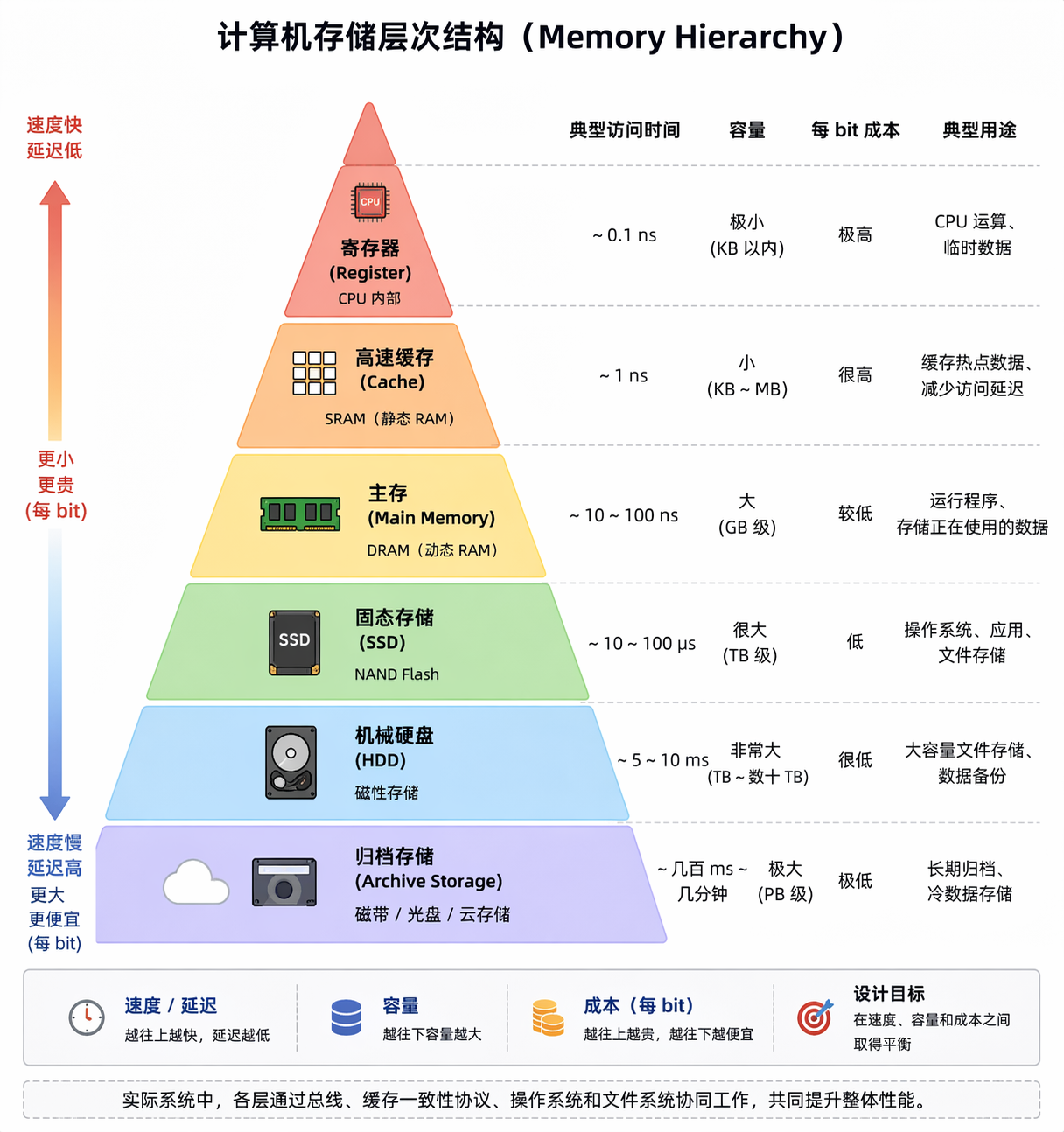
AI Visual Insight: This diagram compares multiple storage and memory technologies in a layered or matrix view across speed, capacity, cost, and whether they retain data after power loss. It clearly illustrates the classic memory pyramid: the closer a technology is to the CPU, the faster it is, the smaller its capacity, and the higher its cost; the closer it is to the persistence layer, the larger its capacity and the lower its speed. This framing helps explain the system role of registers, cache, DRAM, Flash, and external storage devices.
Selection becomes easier when you first answer where code boots from, where data is written, and what memory the system runs on
When designing embedded or general systems, do not start by memorizing parameter tables. Start by separating responsibilities instead: for boot code, evaluate NOR or SPI Flash first; for the main data drive, prioritize NAND-based packaged storage; for runtime memory, focus on the DRAM family; for ultra-low-latency caching, rely on SRAM.
Once you split the problem into boot, runtime, and persistence, memory selection shifts from fragmented memorization to structured decision-making.
FAQ
1. Why do many embedded devices store the Bootloader in SPI NOR?
Because SPI NOR supports fast random reads and can be accessed directly by the CPU during the earliest boot stages, making it suitable for executing boot code. At the same time, it uses fewer pins and keeps hardware cost and design complexity under control.
2. Why can’t NAND Flash execute code directly like NOR Flash?
Because NAND is optimized around page reads and block erases, and it does not provide the byte-addressable random access or stable execution model that NOR offers. It is better suited for large-capacity data storage than direct instruction execution.
3. What is the essential difference between eMMC, UFS, and SSD?
All three are usually built on top of NAND Flash. The main differences lie in controller capability, interface protocol, concurrency model, and performance tier. eMMC targets low-cost designs, UFS targets high-performance mobile systems, and SSD targets high-throughput desktop and server workloads.
Core Summary: This article systematically explains the core differences between volatile and non-volatile memory, with a focus on the operating characteristics, performance trade-offs, and typical use cases of NOR Flash, NAND Flash, SSD, eMMC, UFS, SRAM, DRAM, DDR, and LPDDR. It helps embedded and systems developers quickly build a complete mental model of modern memory technologies.