This article breaks down an FPGA-based BPSK modulation and demodulation system. Its core capabilities include BPSK modulation, AWGN channel simulation, and coherent demodulation, addressing common challenges such as translating communication algorithms into hardware, coordinating multiple modules, and lowering the barrier to simulation-based verification. Keywords: FPGA, BPSK, Verilog.
The technical specification snapshot summarizes the project at a glance
| Parameter | Description |
|---|---|
| Implementation Language | Verilog |
| Hardware Platform | FPGA |
| Development Tool | Vivado 2022.2 |
| Modulation Scheme | BPSK |
| Channel Model | AWGN |
| Input Signal | Binary bitstream i_x |
| Adjustable Parameter | Signal-to-Noise Ratio i_SNR |
| Core Dependencies | Modulator, AWGN module, demodulator |
| Star Count | Not provided in the original source |
The system uses a modular signal chain to validate BPSK transmission and reception
This design focuses on a minimal but functional digital communication link: the transmitter performs BPSK modulation, the middle stage injects interference through a Gaussian white noise channel, and the receiver demodulates and makes symbol decisions to recover the original bitstream. The value of this design lies in mapping communication theory directly into an FPGA-synthesizable structure.
The system fits three common use cases: teaching labs, communication IP prototyping, and early-stage development of low-order modulation links. Compared with moving directly from MATLAB to hardware, this approach offers clearer interfaces, better hierarchy, and easier module-by-module simulation.

AI Visual Insight: This diagram shows the system-level flow, typically including key nodes such as the bit source, BPSK modulator, noise channel, demodulator, and decision output. It emphasizes that the data path is serialized across transmission, channel propagation, and reception, making it easier to identify clock boundaries, bit-width propagation, and inter-module interface relationships.
The top-level signal chain can be abstracted into a three-stage pipeline: transmit, noise injection, and receive
module bpsk_top(
    input               i_clk,
    input               i_rst,
    input               i_x,
    input signed [7:0]  i_SNR,
    output              o_bit
);

wire signed [15:0] o_bpsk;   // BPSK waveform after modulation
wire signed [15:0] o_bpskN;  // Received signal after noise injection

// Transmitter: map the input bit to a phase-reversed signal
bpsk_mod u_mod (
    .i_clk(i_clk),
    .i_rst(i_rst),
    .i_x(i_x),
    .o_bpsk(o_bpsk)
);

// Channel: inject additive white Gaussian noise according to the configured SNR
awgns u_awgn (
    .i_clk(i_clk),
    .i_rst(i_rst),
    .i_SNR(i_SNR),
    .i_din(o_bpsk),
    .o_dout(o_bpskN)
);

// Receiver: perform coherent demodulation and bit decision
bpsk_demod u_demod (
    .i_clk(i_clk),
    .i_rst(i_rst),
    .i_bpsk(o_bpskN),
    .o_y(o_bit)
);

endmodule
This code shows the most important module-level connection in the system, namely how the signal flows from the baseband bitstream through the modulation, channel, and demodulation blocks.
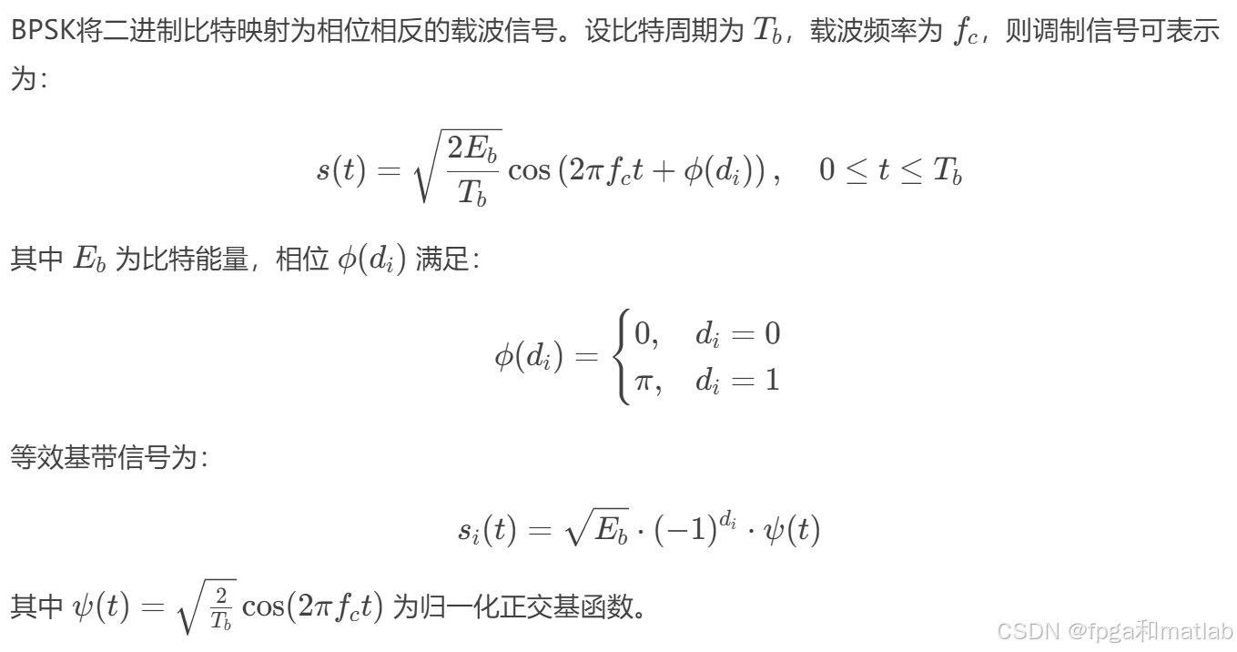
The key to BPSK demodulation is phase decision rather than amplitude recovery
The basic idea of BPSK is to represent binary 0 and 1 with two carrier phase states. Compared with ASK, BPSK is more robust against amplitude disturbances, which gives it better noise immunity in low-SNR environments. That is also why it appears so frequently in foundational digital communication experiments.
At the receiver, the core task of demodulation is not to reconstruct a visually perfect analog waveform, but to correctly determine the phase sign associated with the current symbol. In practical engineering, this is typically achieved through multiplication with a local carrier, low-pass filtering, and threshold-based decision logic.
AI Visual Insight: This figure illustrates the principle of BPSK modulation and demodulation. It typically includes units such as carrier generation, multipliers, filters, and decision logic, highlighting how the receiver performs correlation-based demodulation using a local reference carrier, then extracts the baseband component through filtering and restores the bitstream.
The demodulation flow can be reduced to three steps: multiply, filter, and decide
always @(posedge i_clk or posedge i_rst) begin
    if (i_rst) begin
        bit_out <= 1'b0;
    end else begin
        mix_data <= i_bpsk * carrier_local; // Multiply by the local carrier for coherent detection
        filt_data <= lp_filter(mix_data);   // Apply low-pass filtering to extract baseband energy
        bit_out <= (filt_data >= 0) ? 1'b1 : 1'b0; // Decide the bit based on the sign
    end
end
This pseudocode captures the main signal-processing path inside the demodulator and helps map communication theory into RTL timing logic.
The simulation results verify consistency between the RTL structure and link output
The original material includes an RTL structure diagram and two sets of simulation waveforms. The RTL diagram helps confirm that module instantiation and port wiring are correct, while the waveform plots verify whether key observation points behave as expected, including the modulated output, noisy output, filtered result, and final decision bit.
If i_SNR increases, the received signal should theoretically become closer to the ideal waveform, and the post-filter decision should become more stable. If i_SNR decreases, noise will make decisions near zero crossings more likely to flip. This is the basic observation framework for evaluating bit-error performance.
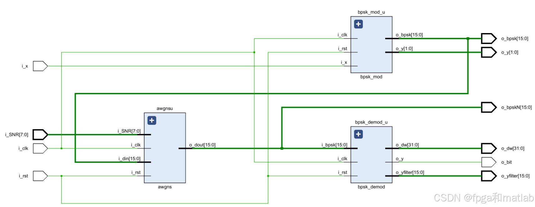
AI Visual Insight: This image shows the RTL hierarchy of the system, with submodules such as the modulator, noise module, and demodulator instantiated under the top-level module. It helps developers check functional partitioning before synthesis, port directions, bit-width compatibility, and consistency of internal signal naming.
The original top-level program exposes the key observation ports
module bpsk_top(
    input i_clk,
    input i_rst,
    input i_x,
    input signed [7:0] i_SNR,
    output signed [1:0]  o_y,
    output signed [15:0] o_bpsk,
    output signed [15:0] o_bpskN,
    output signed [31:0] o_dw,
    output signed [15:0] o_yfilter,
    output o_bit
);

// Each output port is used to observe intermediate results
// during modulation, noise injection, and demodulation
// This is critical for testbench waveform analysis
endmodule
This interface design shows that the author focuses not only on the final bit output, but also preserves multiple internal nodes for debugging and instructional visualization.
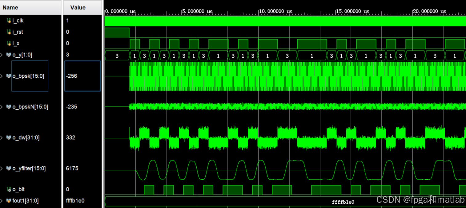
AI Visual Insight: This simulation plot most likely shows the timing relationship among the transmitted bits, the modulated waveform, and the receive chain. Developers can use it to verify whether symbol transitions align with the input bits and whether the waveform still retains decodable phase characteristics after noise injection.
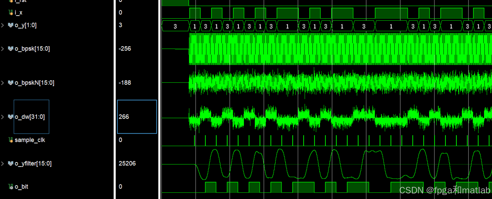
AI Visual Insight: This waveform further reflects the relationship between the filtered demodulator output and the final decision bit. If the filtered result maintains a clear positive or negative polarity around the sampling points, the demodulation chain has usable decision margin.
Reproducing the design depends on observability and parameterization
From an engineering perspective, the strength of this project is not algorithmic complexity but structural completeness. It already provides the three essential properties required for a communication link experiment: it runs, it is tunable, and it is observable. In particular, the i_SNR input enables the same testbench to quickly cover multiple channel conditions.
If you want to extend the project, three directions are the most natural: add carrier synchronization, include a bit-error-rate statistics module, and scale the design to QPSK or higher-order modulation. That would allow the project to evolve from a teaching-oriented demonstration into a more realistic digital receiver validation platform.
A simplified testbench is enough to verify end-to-end link connectivity
initial begin
    i_clk = 0;
    i_rst = 1;
    i_x   = 0;
    i_SNR = 8'd20; // Set the SNR to 20 dB
    #100;
    i_rst = 0;

    repeat(16) begin
        #20 i_x = ~i_x; // Toggle the input bit periodically to observe modulation and demodulation results
    end
end

always #5 i_clk = ~i_clk; // Generate the system clock
This test code drives the clock, reset, and input bitstream, making it the smallest practical stimulus template for validating BPSK link connectivity.
The downloadable resources can be used directly to reproduce the Vivado project
The original material states that the complete runnable code has been uploaded to CSDN, using Vivado 2022.2, along with a step-by-step video guide. That means the project is positioned more as a directly reproducible teaching design than as a purely conceptual example.
For developers who want to get started quickly, the recommended workflow is to complete behavioral simulation first, then inspect post-synthesis timing and resource utilization, and finally adjust the sampling rate, carrier parameters, and filter coefficients according to the target FPGA board clock conditions.
FAQ
1. Who is this BPSK FPGA project best suited for?
It is well suited for engineers and students learning digital communications, Verilog design, or Vivado simulation. It covers the three core stages of the signal chain—modulation, channel modeling, and demodulation—which makes it useful for building a complete end-to-end understanding.
2. What problems arise without carrier synchronization?
If the transmitted carrier and the local carrier have a frequency offset or phase mismatch, coherent demodulation performance will degrade. In severe cases, the decision boundary may drift and bit errors may increase. This project is better treated as a foundational version that comes before carrier synchronization is added.
3. How can you tell whether the simulation results are correct?
Focus on four types of signals: the input bitstream, the modulated waveform, the waveform after noise injection, and the demodulated decision output. If the output bits largely match the input under high SNR and the intermediate filtered result maintains a stable sign, the link is functioning correctly.
Core Summary: This article reconstructs an FPGA-based BPSK modulation and demodulation project, covering the system architecture, modulation and demodulation principles, AWGN channel injection, RTL top-level connections, and simulation results. It is a solid starting point for Vivado and Verilog-based communication link development and reproduction.